Saw Singulation – Process Engineer
In the realm of semiconductor manufacturing, where precision is paramount and the tiniest error can lead to significant consequences, the process of saw singulation stands as a crucial step in bringing intricate designs to life. As chips become smaller and more complex, the need for impeccable accuracy in separating individual semiconductor units from a larger substrate grows ever more pressing. Enter the saw singulation process engineer, whose expertise lies in orchestrating this delicate dance of cutting-edge technology and meticulous execution.
Understanding Saw Singulation
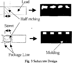
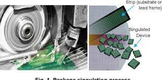
Before delving into the role of a process engineer in saw singulation, it’s essential to grasp the fundamentals of the process itself. Saw singulation is the method by which semiconductor wafers, often containing numerous individual chips or integrated circuits, are separated into distinct units. This separation allows for the individual packaging and integration of each chip into electronic devices such as smartphones, computers, and IoT devices.
The process typically involves the use of precision saws equipped with diamond blades, which make extremely fine cuts through the semiconductor material. These saws can operate with astonishing accuracy, often achieving cuts as thin as a few micrometers. However, achieving such precision requires not only advanced machinery but also meticulous planning and execution guided by knowledgeable process engineers.
The Role of a Saw Singulation Process Engineer
At the heart of the saw singulation process lies the expertise of the process engineer. These professionals are tasked with overseeing every aspect of the singulation process, from initial planning to final implementation. Their responsibilities encompass a wide array of tasks, each crucial to ensuring the success and efficiency of the operation:
1. Process Design and Optimization:
Process engineers are responsible for designing the optimal singulation process for a given semiconductor design. This includes selecting the appropriate sawing parameters such as blade speed, feed rate, and cutting depth to achieve the desired results while minimizing waste and defects. Through careful analysis and experimentation, they fine-tune these parameters to maximize yield and throughput.
2. Equipment Selection and Maintenance:
Choosing the right sawing equipment is paramount to the success of the singulation process. Process engineers work closely with equipment vendors to select saws that meet the specific requirements of the semiconductor design. They also oversee the maintenance and calibration of these machines to ensure they operate at peak performance, minimizing downtime and ensuring consistent results.
3. Quality Control:
Maintaining strict quality control standards is essential in semiconductor manufacturing, and saw singulation is no exception. Process engineers develop and implement rigorous inspection protocols to detect defects such as chipping, cracking, or misalignment early in the process. By identifying and addressing these issues promptly, they help prevent costly scrap and rework downstream.
4. Yield Enhancement:
Improving yield – the ratio of usable chips to total chips manufactured – is a constant goal in semiconductor fabrication. Process engineers play a vital role in this endeavor by identifying and addressing root causes of yield loss, such as sawing-induced damage or material defects. Through careful analysis and process optimization, they strive to maximize the number of viable chips produced per wafer.
5. Process Integration:
The singulation process is just one step in the larger semiconductor manufacturing workflow. Process engineers collaborate closely with colleagues across various departments, including lithography, etching, and packaging, to ensure seamless integration of the singulation process into the overall fabrication process. This coordination is essential for maintaining efficiency and consistency across the entire production line.
Challenges and Innovations
While saw singulation has long been a staple of semiconductor manufacturing, it is not without its challenges. As semiconductor designs continue to shrink and become more complex, the demands placed on the singulation process – and by extension, the engineers overseeing it – continue to increase. Some of the key challenges facing saw singulation process engineers include:
1. Miniaturization:
As semiconductor features shrink to ever-smaller dimensions, the tolerances for saw singulation become increasingly tight. Process engineers must contend with challenges such as maintaining sufficient chip strength and minimizing edge chipping while cutting through micron-scale structures.
2. Advanced Materials:
The rise of new materials such as gallium nitride (GaN) and silicon carbide (SiC) presents new challenges for saw singulation. These materials can be harder and more brittle than traditional silicon, requiring specialized cutting techniques and tooling to achieve clean, precise cuts.
3. Cost Pressures:
Semiconductor manufacturing is a highly competitive industry, and cost considerations loom large. Process engineers must balance the need for high-quality results with the imperative to minimize manufacturing costs, often through optimization of process parameters and equipment utilization.
4. Environmental Impact:
The semiconductor industry’s environmental footprint is a growing concern, prompting efforts to reduce waste and energy consumption. Process engineers play a role in this effort by exploring alternative materials and techniques that minimize environmental impact without compromising performance.
In the face of these challenges, saw singulation process engineers are continually innovating to develop new techniques and technologies that push the boundaries of what is possible. Whether through advancements in sawing equipment, novel process designs, or innovative materials, these professionals are driving the evolution of semiconductor manufacturing forward.
Conclusion
Saw singulation is a critical step in semiconductor manufacturing, requiring a delicate balance of precision, expertise, and innovation. The role of the saw singulation process engineer is central to ensuring the success of this process, from initial design to final implementation. By leveraging their knowledge and skills, these professionals help bring cutting-edge semiconductor designs to life, enabling the continued advancement of technology in industries ranging from consumer electronics to automotive and beyond. As semiconductor technology continues to evolve, the importance of saw singulation – and the engineers who oversee it – will only continue to grow.